


AI Smart Terminal Solution
With the advancement of AI smartphones and other terminal products, increasingly complex structure, and miniaturized features such as holes, circuit, and dielectric thickness.
Mainstream smartphones adopt high-end HDI boards; while high-end models adopt anylayer HDI or substrate-like PCBs. Typical manufacturing processes include the subtractive process (Tenting L/S ≥ 35/35 μm) and the modified semi-additive process (mSAP L/S ≤ 30/30 μm). Next-generation smartphone motherboards are shifting from traditional FR-4 materials to RCC and ABF, meet higher-density wiring needs. In addition, flexible printed circuits (FPCs) serve as critical 3D interconnection inside smart device supports more functions, with multi-layer design and high density as the main development trend.
In response to the technological trends in the smartphone industry, Han's CNC provides diversified product solutions to empower the industrial technological upgrading.

Core Technology&Main Products
-
01
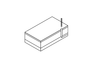
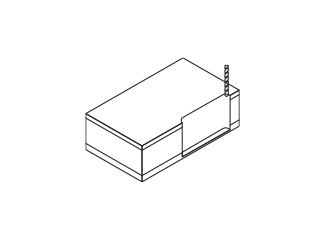
Drilling
 01More
Drilling
As HDI core boards adopt finer feature sizes such as smaller via diameters, higher hole density and reduced annular rings, higher standards are demanded for processing accuracy and efficiency. Han's CNC delivers differentiated solutions for various types of holes: mechanical drilling machines equipped with high-speed spindles are used for core boards through vias, enabling efficient processing of micro-diameter holes; for blind vias and X-vias, both CO₂ laser and ultra-fast laser solutions are offered to meet the varying production process requirements.
-
02
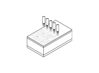
Pattern Transfer
02MorePattern Transfer
Driven by the growing I/O count of smartphone processor chips, finer BGA pitch and ever-increasing HDI wiring density. Han's CNC has launched a fine-line Laser Direct Imaging (LDI) system, with optimized optical path design and ultra-high dry film resolution. It can satisfy the expansion/contraction and segmentation processing in various modes, greatly improve the pattern positioning accuracy.
-
03
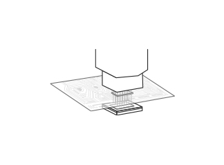
Routing
03MoreRouting
Driven by increasingly stringent overall dimensional tolerance requirements for smartphone HDI, the multi-panel design poses challenges to the final board depaneling and routing. Han's CNC provides high-accuracy and high-stability products to address these challenges, and offers separate CCD control models for deformed boards and products with ultra-high positioning accuracy requirements.
-
04
Quality Control
04MoreQuality Control
The manufacturing challenges of smartphones varies greatly. Factors such as solder joint density, pad size, and production risks all affect the selection of electrical performance testing equipment. With the continuous improvement of overall testing density, Han's CNC provides Universal 25mil Grid Micro-probe Testing Machine and High-Precision Micro-probe Testing Machine, which meet the requirements of 2/4-wire testing respectively.
-
05
Packaging
05MorePackaging
Han's CNC provides a fully automatic sorting and packaging line to realize finished product packaging that is scratch-resistant, contamination-free, and prevents material mixing.
They are all partnering with us.
We serve leading PCB enterprises worldwide, covering the top 100 PCB manufacturers in China, and gaining customer recognition with technology and quality.


Ranking is not in any particular order


