


High speed optical module solution
The optical module PCB technology developed toward high precision and high integration as driven by the transition of data centers to 400G/800G/1.6T/3.2T optical modules.The proportion of any-layer HDI and Substrate-Like PCBs (SLP) over 12 layers keeps rising steadily. To ensure the integrity of high-rate signal transmission, and the miniaturized PCBs characteristic parameters, Han's CNC provides leading full-process solutions to meet the processing demands of high-speed materials and more complex structures, empowering the cost control and yield improvement of advanced HDI processes for optical module PCBs.

Core Technology&Main Products
-
01
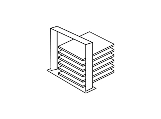
Lamination
 01More
Lamination
Driven by advanced DSP chip processes, the 800G+ optical modules are evolving toward a more refined andcomplex technical architecture, as PCBs transition from Anylayer HDI to Substrate-Like PCBs (SLP) with higher layer counts, ultra-thin copper foils and dielectric layers. Han's CNC provides a customized solution for high-precision alignment, strict temperature and pressure control, advanced material matching, and complex structural processes for multiple lamination of thinner materials
-
02
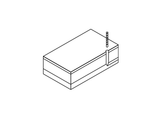
Drilling
02MoreDrilling
The increasing proportion of anylayer HDI adopted in 800G+ high-speed optical modules. Moreover, with the advancement of DSP chips, mSAP-Substrate-Like PCBs have gradually become the mainstream, leading to further miniaturization of blind via diameter and increasing density. Han's CNC provides an ultra-fast laser drilling solution featuring less thermal effects, higher accuracy, and better quality, helping to improve the yield of high-end HDI products in the downstream industry.
-
03
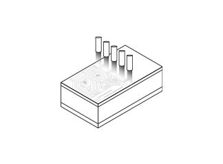
Pattern Transfer
03MorePattern Transfer
The requirement on optical module circuit patterns tolerance is high to support the high-speed signal transmission stability. Moreover,increasing wiring density poses challenges to the minimum resolution capability of exposure machine.Han's CNC provides more precise pattern control, higher alignment accuracy, and multi-segmentation technology for fine circuit processing, ensuring the dimensional consistency of circuits in the mSAP process.
-
04
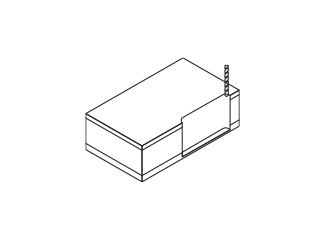
Routing
04MoreRouting
With increasingly stringent dimensional accuracy requirements for optical module bonding pads and edge connectors,coupled with the demands for heat dissipation and embedded miniaturization, requires high accuracy and stability for profile and cavity processing. Han's CNC provides high-speed spindle CCD mechanical and ultra-fast laser routing solutions for various specifications, ensure high-quality processing tolerances of bonding pads and finished panel separation.
-
05
Quality Control
05MoreQuality Control
The inspection machine is necessary for both the PCB manufacturing process and the final finished products quality control; as the increasing requirements for feature tolerance and signal integrity, higher standards are put forward for the reliability of inspection equipment. Han's CNC provides more refined product solutions for quality control, including high-resolution optical inspection machines, appearance inspection machines, as well as large-platform universal testing machines with high electrical performance standards.
They are all partnering with us.
We serve leading PCB enterprises worldwide, covering the top 100 PCB manufacturers in China, and gaining customer recognition with technology and quality.


Ranking is not in any particular order


